欧美一级日韩一级,国产精品xxx,午夜毛片视频,黄色片在线免费,国产h在线观看,中文一区二区视频,又大又硬一进一出做视频

Xiamen SAN-U Optronics Co., Ltd.
  • SAN-U Optronics: Self-developed chip mass production and sales of detection device series products reach a new high!
    SAN-U Optronics: Self-developed chip mass production and sales of detection device series products reach a new high! Dec 01, 2025
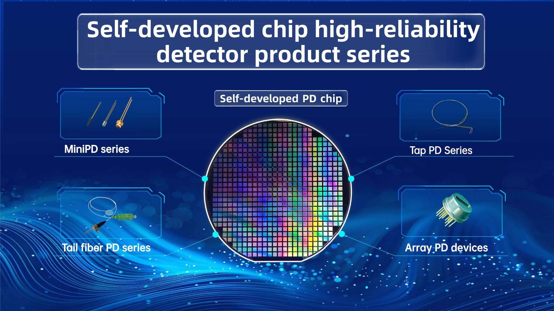
    Self developed chip high reliability detector product matrix SAN-U Optronics: Heavy Release of Self Developed Photodiode Chips and Series Devices Recently, SAN-U Optronics' self-developed Photodiode chip and series of devices were officially released, marking our company's promotion of domestic substitution of key optical devices in the field of optical communication. As a key link in the optical communication industry chain, PD chips are known as the "translator of optical signals", and their performance directly determines the transmission efficiency and reliability of optical communication systems. Based on the technological breakthrough of self-developed PD chips, SAN-U Optronics has launched four major product matrices: MiniPD series, tail fiber PD (adhesive/laser welding), TapPD series, and arrayed PD devices. With the dual advantages of "diversified product types+domestic chip substitution", the products are mainly used in the fields of fiber amplifiers, optical power meters, optical signal data transmission, and optical sensing. Self developed Photodiode chip and series device product Series ① SAN-U self-developed Photodiode chip The Photodiode self-developed chip adopts a PIN structure design, which has ultra-low dark current, high reliability, and low voltage operation characteristics. The working temperature range covers -40~+85 ℃, meeting the stable operation requirements in extreme environments. ② Mini Photodiode series The Mini Photodiode series products have a minimum diameter of 1.2mm and are equipped with high-precision and highly reliable gas sealing technology. While the size is reduced, the devices still have high performance and reliability. Mainly used in high-speed optical communication (high-speed fiber optic transceiver modules, fiber optic amplifiers), optical sensing systems (oil well monitoring, power equipment temperature measurement, perimeter security), industrial and military, aerospace and other high-end application fields. ③ Photodiode with pigtail series The SAN-U Optronics  PD with pigtail series products have constructed a product matrix covering multiple scenarios through process differentiation design, using two packaging processes of adhesive and laser welding to accurately match different application needs. The adhesive process relies on an automated mass production system to achieve low-cost and high-efficiency production, especially suitable for cost sensitive large-scale scenarios such as optical communication equipment; The laser welding process uses gold tin eutectic welding technology to form stable connections through intermetallic compound bonding, which can meet the strict reliability requirements of industrial applications. This product can be widely used in fields such as optical communication and fiber optic sensing. ④ The TapPD series The TapPD series of products integrates a splitter and a detector into a compact package, enabling real-time, non-destructive sampling and monitoring of optical signals without interrupting the main optical path signal transmission, thus ensuring stable signal transmission. The products are primarily used in fiber optic communication transmitters, fiber optic amplifiers, optical power meters, medical lasers, and other fields. ⑤ The ArrayPD device series   The ArrayPD device series, through its array design, achieves higher detection efficiency and faster response speed. This product is suitable for high-end applications such as lidar and medical imaging, providing strong technical support for the development of related industries. CORE PARAMETERS COMPARISON After extensive testing and comparison between SAN-U's self-developed Photodiode chip and well-known foreign chips, as well as customer testing and feedback, it is found that SAN-U's chip has lower dark current compared to foreign Photodiode chips, while other parameters and performance are on par or better than those of foreign chips.   LOCALIZATION ACCELERATES SELF-CONTROL SAN-U Optronics  has been deeply involved in the field of optoelectronics for over 20 years, with a full industrial chain layout of "chip design - packaging and testing - module application". Currently, with the accelerated construction of AI computing power centers, the accelerated layout of in-vehicle optical communication and 10-gigabit networks, the demand for optical communication devices is experiencing explosive growth. SAN-U Optronics  is precisely positioning itself to seize these market opportunities.   Fully leveraging the industrial advantages of Xiamen's local optoelectronic semiconductors, we have linked up with chip manufacturing enterprises around Xiamen to promote regional industrial collaboration. Downstream, we provide cost-effective products to downstream manufacturers, playing a role in strengthening and complementing the supply chain in the field of optoelectronic semiconductors.  
  • SAN-U Optronics | Reveal the optical communication device production line
    SAN-U Optronics | Reveal the optical communication device production line Jul 07, 2025
            Reveal the optical communication                  device production line                  SAN-U Optronics 10,000 clean room                                SAN-U Optronics           10,000 clean standards, casting high-speed optical communication core cornerstone   In the era of 5G/6G and Al arithmetic outbreak, every microsecond of optical signal transmissioncarries the accurate delivery of massive data. As a supplier of core devices for high-speed opticacommunication, San-U Optronics builds a precision manufacturing environment for semiconductor lasersdetectors and optical transceiver components with 10,000 cleanliness standards to ensure the efficient andstable operation of communication links.
  • Methane Laser Sensor: Efficient and Accurate Gas Detection Solution
    Methane Laser Sensor: Efficient and Accurate Gas Detection Solution Nov 22, 2024
    Introduction: Gas detection has become increasingly important in modern industry and environmental monitoring. One of the key tasks is to detect methane gas concentration, as methane is a common greenhouse gas that has significant impacts on climate change and environmental safety. In order to provide efficient and accurate gas concentration detection solutions, methane laser sensors have emerged. This article will introduce the principle, advantages, and application areas of methane laser sensors. Principle: The methane laser sensor is based on Laser Absorption Spectroscopy (TDLAS) technology. It uses a laser beam with a specific wavelength of 1653.7nm to measure the absorption spectrum of methane molecules in the gas being tested. By measuring changes in absorption intensity, the concentration of methane gas can be derived. This technology has the characteristics of high sensitivity, fast response, and high resolution.                   Advantages: Compared to traditional gas sensors, methane laser sensors have the following advantages: a) High sensitivity: Methane laser sensors have high sensitivity to methane gas and can detect extremely low concentrations of methane, typically in the ppm (parts per million) or ppb (parts per billion) range. b) Accuracy: Laser absorption spectroscopy technology can provide highly accurate measurement results, reducing false alarms and errors. c) Real time monitoring: The methane laser sensor has real-time monitoring function, which can quickly respond to emergency situations such as methane leakage and improve safety. d) Long lifespan: The methane laser sensor uses a reliable laser light source, which has a long service life and stability. Application areas: Methane laser sensors have a wide range of applications in various fields, including but not limited to: a) Industrial safety: Methane laser sensors can be used for monitoring methane leaks in fields such as petroleum, natural gas, and chemical engineering, providing rapid response and ensuring the safety of the working environment. b) Environmental monitoring: Methane is a greenhouse gas that has a significant impact on climate change. Methane laser sensors can be used for environmental applications such as atmospheric monitoring and greenhouse gas emission monitoring, helping to assess and reduce methane emissions. c) Mine safety: Methane is a common combustible gas that can easily cause explosions during mining operations. Methane laser sensors can be used for methane gas detection and alarm, ensuring the safety of miners. d) Gas energy detection: Methane is the main component of natural gas, and methane laser sensors can be used for natural gas exploration and downhole operations, providing key gas concentration information. Conclusion: Methane laser sensors, as an efficient and accurate gas detection solution, are widely used in industrial and environmental fields. Its high sensitivity, accuracy, and real-time monitoring capabilities make it an important tool for improving safety and environmental monitoring levels. With the continuous advancement of technology, methane laser sensors will continue to develop and play a role in more fields, promoting sustainable development and environmental protection.
  • New industrial park helps product transformation, 400G/800G OEM services debut in the industry
    New industrial park helps product transformation, 400G/800G OEM services debut in the industry Sep 20, 2023
    During the 2023 CIOE, Xiamen SAN-U Optronics Co., Ltd. (referred to as SAN-U Optronics), a provider of high-speed semiconductor lasers/detectors and optical transceiver components, showcased a series of 25G/50G/100G optical devices and COB optical engine products, which are widely used in fields such as cloud computing, optical communication, fiber to the home, sensing and detection, and LiDAR. Dr. Li Ling, Chairman of Sanyou Optoelectronics, was interviewed by Xunshi Optical Communication Network on site. She stated that the company mainly exhibited three major application products, data communication, optical sensing, and airtight packaging, at this year's CIOE China Optical Expo, showcasing the leading intelligent manufacturing platform for optoelectronic devices in China. The products have received high-end attention from industry customers. In terms of data communication, SAN-U Optronics has successfully expanded its 400G/800G OEM services based on its existing high-speed optical engine technology product foundation. With the explosion of AI computing power connectivity in 2023, the demand for 800G optical communication has exceeded everyone's expectations. The entire industry is preparing sufficient materials for the delivery of 800G products, among which 400G/800G high-speed chips are still the most scarce key materials in the supply chain, bringing a new round of development opportunities for domestic optoelectronic chips. After more than 20 years of development, Sanyou Optoelectronics' optoelectronic chip packaging platform has been widely certified by the industry and customers. It can provide industry-leading chip packaging services and help accelerate the industrialization of domestic chips. In terms of optical sensing, SAN-U Optronics mainly researches and manufactures laser and MEMS sensor products. The company team has conducted in-depth research and development in this new field, and has achieved market breakthroughs in a series of products such as LiDAR, methane gas detection lasers/detectors, MEMS micro pump bio chip packaging and bio printing chip products, and fast detection chip products, receiving good customer feedback. In the context of weak traditional single market, the sensing market has provided strong performance support for the company. In addition, in terms of the application of airtight packaging technology, SAN-U Optronics has successfully introduced airtight packaging technology into the field of third-generation semiconductor materials, mainly in the new energy industry dominated by silicon carbide (SiC). With the prosperity of the new energy vehicle industry, silicon carbide has become the hottest semiconductor material, and related domestic silicon carbide materials and devices are rapidly rising.

Need Help? Chat with us

leave a message
For any request of information or technical support, fill in the form. All fields marked with an asterisk * are required.
Submit

Home

Products

whatsApp

contact

富蕴县| 广灵县| 上林县| 广德县| 巴彦淖尔市| 崇仁县| 桃源县| 茌平县| 准格尔旗| 贡山| 古浪县| 菏泽市| 巩义市| 长葛市| 武胜县| 布尔津县| 图们市| 乐陵市| 揭西县| 平凉市| 和田市| 东兴市| 北京市| 襄汾县| 思南县| 札达县| 柳州市| 缙云县| 东乡族自治县| 巧家县| 天祝| 扎兰屯市| 涞水县| 洞头县| 兰考县| 微博| 昌图县| 镇康县| 和静县| 万荣县| 清流县|